
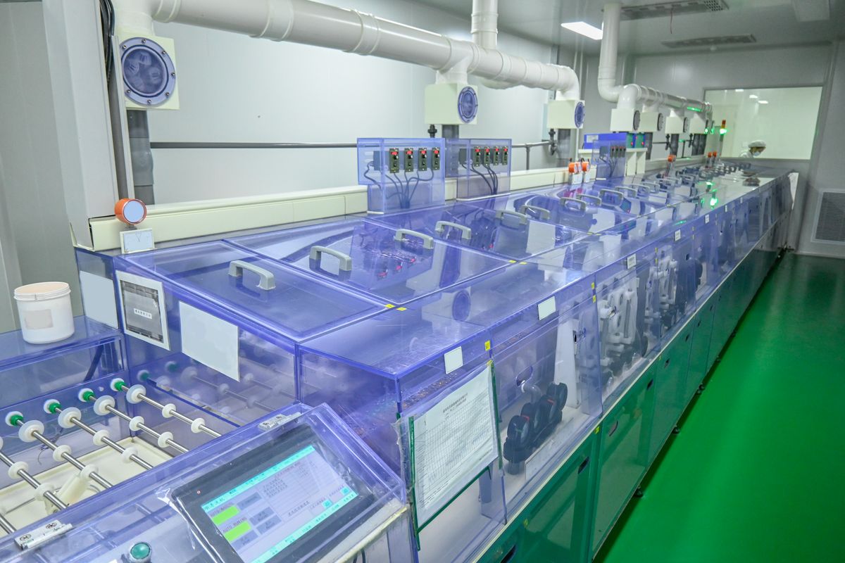
CleaningGlass Washing Machine
Fully automatic glass substrate cleaning line with ultrasonic, brush and DI-water rinse and hot-air drying, ensuring substrate cleanliness meets thin film deposition requirements.
Redirecting in 5s. 1688.com is a Chinese-language B2B platform.
Photovoltaic self-power for low-power electronics, from smart home to outdoor portable energy. No battery swaps, no wiring.
Company updates and important notices.
No announcements yet.
Hunan Xuyu New Energy Technology Co., Ltd. was founded in 2018 and is located in the Changde National High-tech Zone, Hunan. It is a high-tech enterprise focused on R&D and manufacturing of amorphous silicon thin film solar cells and high-efficiency thin film solar cells, supported by a professional technical and management team.
In 2025, the company completed a 22-mu high-efficiency thin film solar materials industrial park, expanding into high-efficiency thin film solar.
On the technology and manufacturing side, the company operates a-Si thin film solar cell production equipment and processes, with in-house R&D and design capability for core equipment and control over key production steps.
On the quality side, the company has established a quality control system and is certified to ISO9001 and ISO14001. Products comply with RoHS and REACH.
Hunan factory established
Photovoltaic power supply for ETC devices
New production line launched
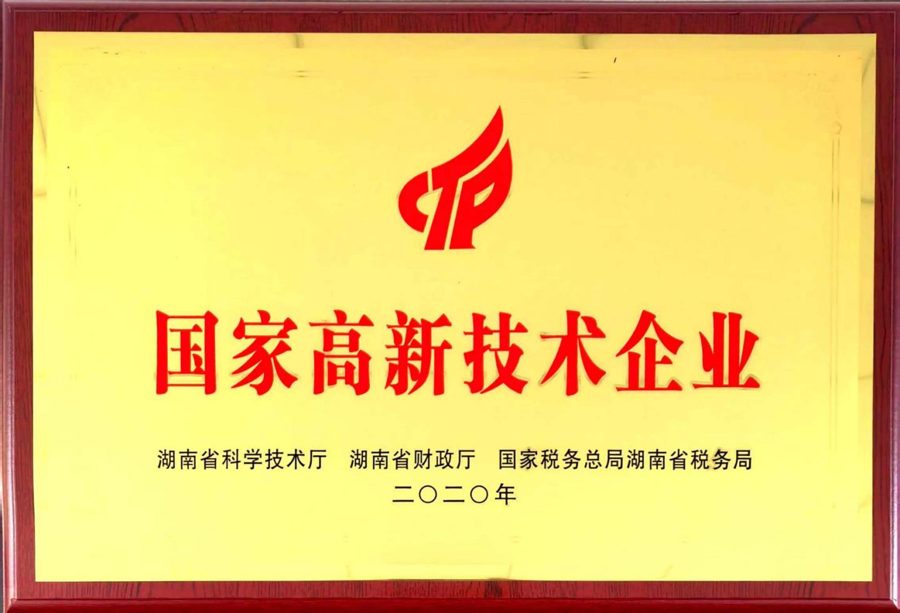
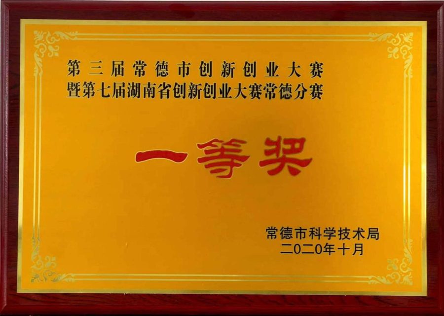
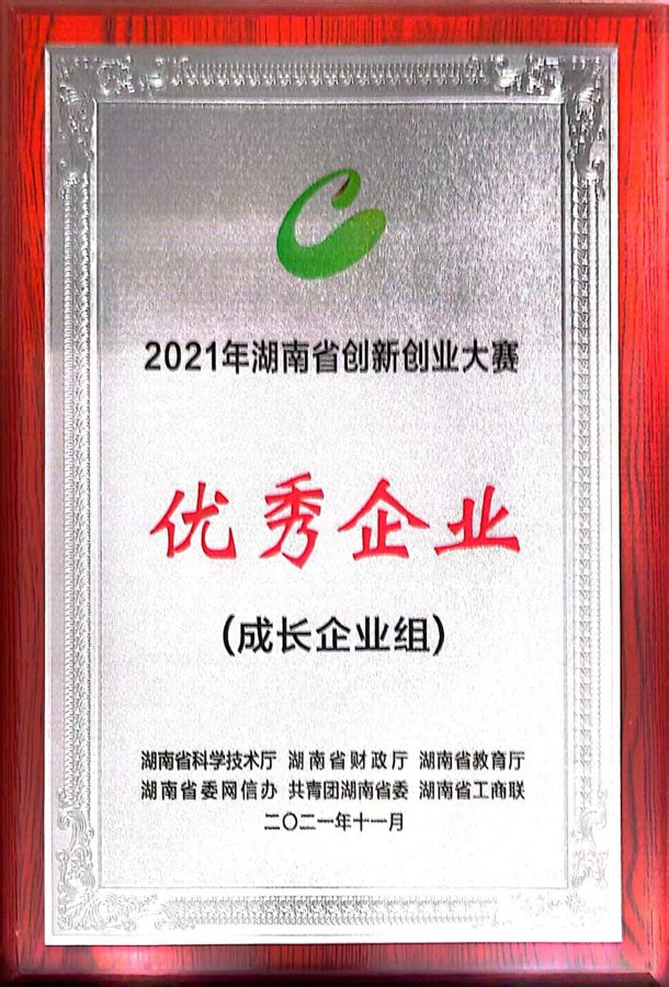
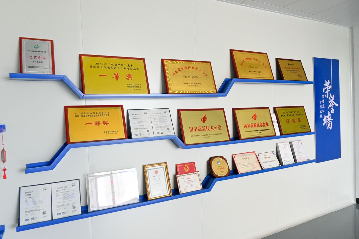
Hunan S&T Innovation Excellence Award; Changde S&T Innovation First Prize
Breakthrough in special-shaped products
High-efficiency cell development begins
Breakthrough in core high-efficiency cell technology
New industrial park completed; high-efficiency thin film cell layout
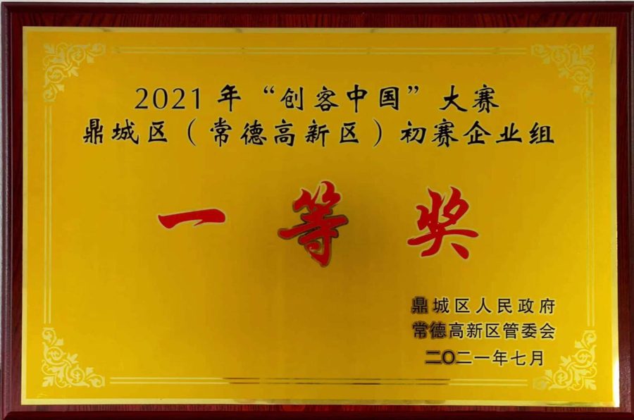
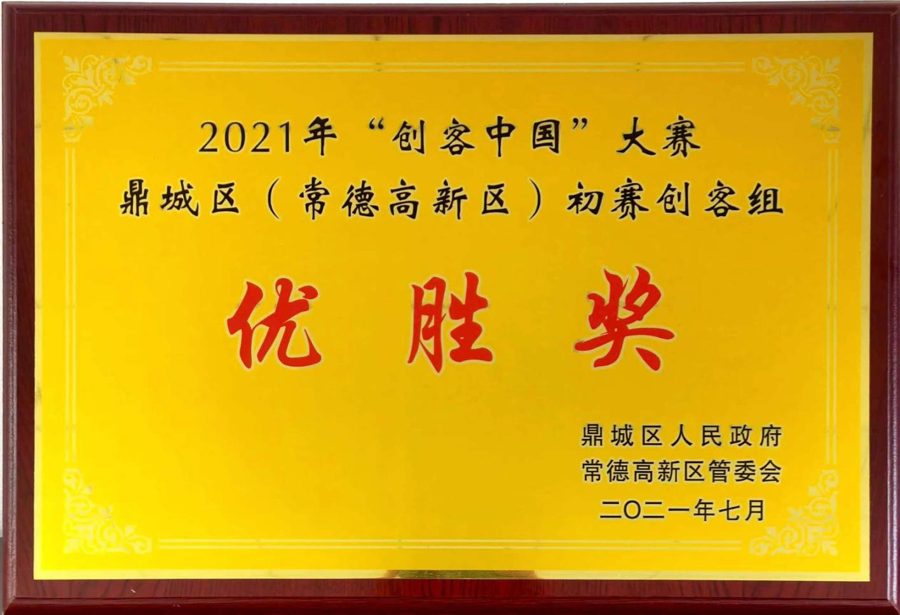
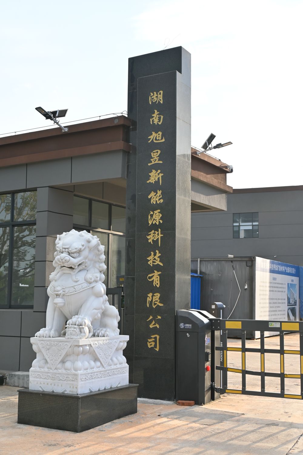
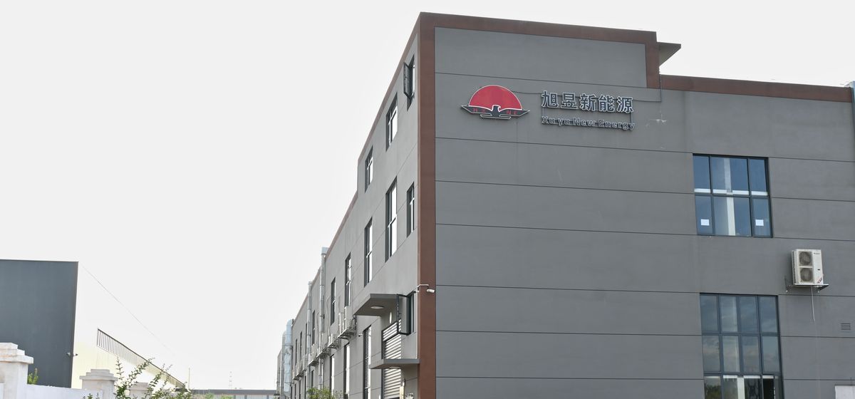
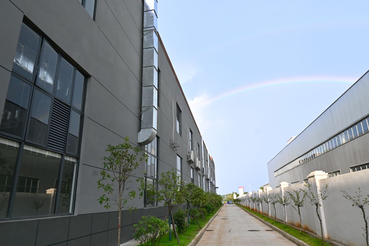
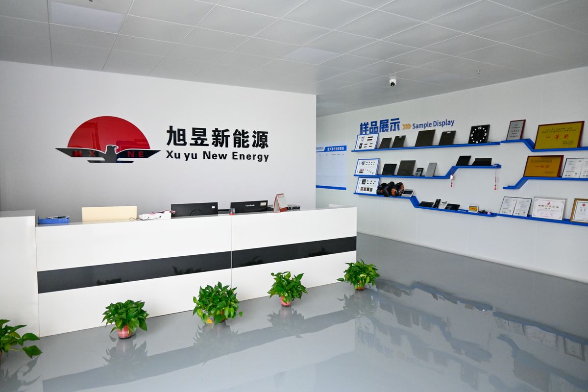
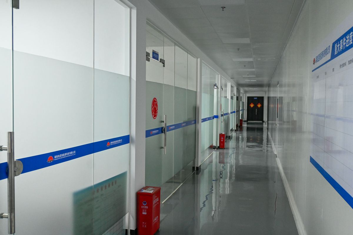
A modern production base with Class 1000 cleanrooms and automated equipment, covering the full process from substrate cleaning to testing and sorting.
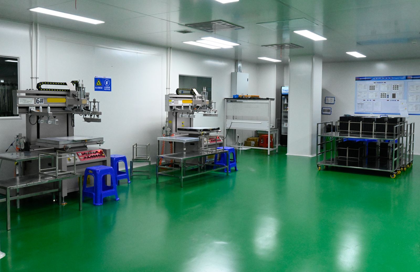
Spanning 7,000 m², the base is equipped with modern thin film solar cell production lines, Class 1000 cleanrooms and automated production equipment.
In 2025, the high-efficiency thin film solar materials park was completed, further expanding R&D and manufacturing capability for high-efficiency thin film cells.
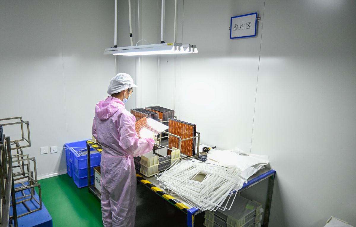
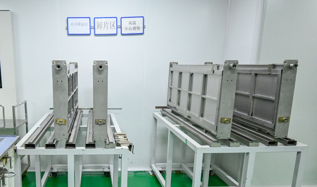
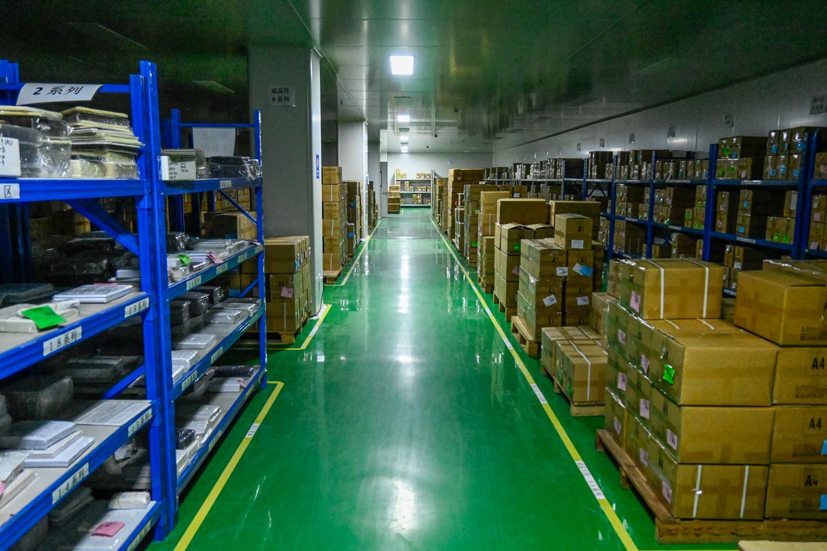
Fully automatic glass substrate cleaning line with ultrasonic, brush and DI-water rinse and hot-air drying, ensuring substrate cleanliness meets thin film deposition requirements.
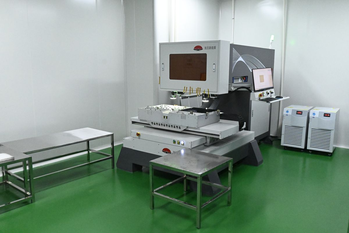
Three laser scribing steps are core to thin film cells: P1 TCO, P2 silicon, P3 back electrode, dividing the continuous film into series-connected sub-cells.
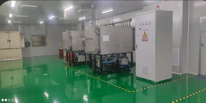
Uses plasma to excite reaction gases in a vacuum chamber, depositing a-Si PIN layers on glass substrates with precise control of film thickness and doping.
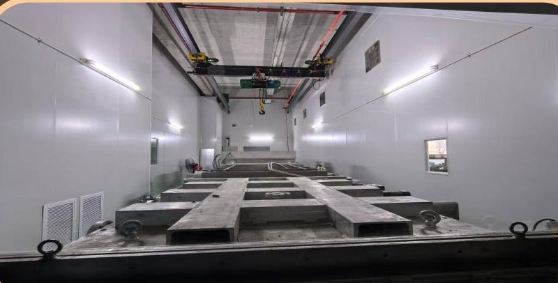
Prepares back electrodes and metal reflection layers by magnetron sputtering. Dense, well-adhered films provide good electrical contact and light reflection.
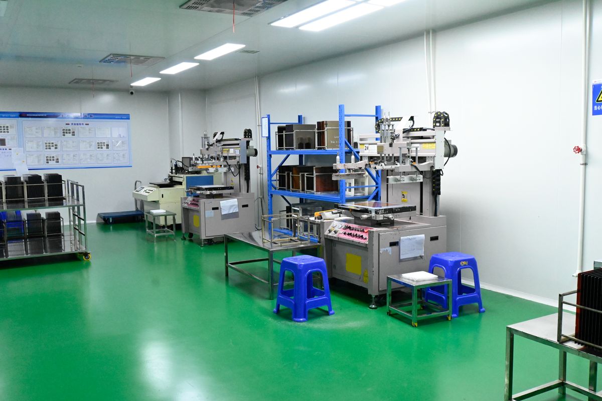
High-precision screen printing of bus electrodes and leads, with CCD vision alignment and ±10 μm repeat positioning accuracy.
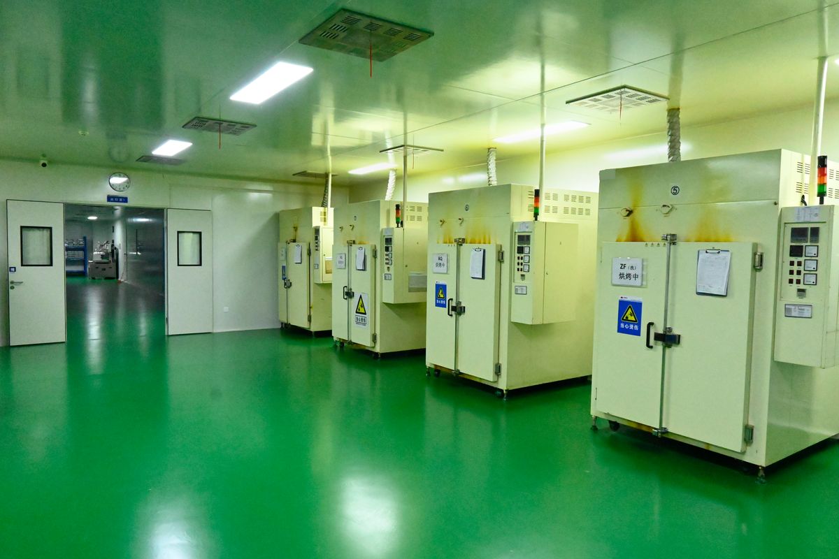
Fast curing oven with precise temperature control, used for annealing and curing functional layers after PECVD to stabilize film quality.
Highlighted steps are laser processes (P1–P4) that divide the continuous film into series-connected sub-cells.
a-Si is deposited by PECVD at relatively low temperature on glass or flexible substrates, suited to powering low-power electronics under indoor low light.
Starts generating power under low indoor illuminance.
Photoactive film only 1–2 μm thick, about 1% of crystalline silicon.
Flexible products under 0.2 mm thick with bending radius below 2 cm.
Low-temperature PECVD deposition with lower manufacturing energy use.
| Dimension | Crystalline Si (c-Si) | Amorphous Si (a-Si) |
|---|---|---|
| Silicon thickness | 180–200 μm | 1–2 μm, thin film deposition |
| Module efficiency | 20–24% | 6–10% (single junction) |
| Indoor low-light response | Weaker | Stronger, suited to low illuminance |
| Mechanical form | Rigid, rigid packaging | Can be flexible |
| Process temperature | >1000 ℃ | ~200 ℃ |
| Typical use | Ground-mount & rooftop PV | Indoor low light, consumer electronics, IoT sensors |
The two technologies serve different scenarios and are not substitutes. Figures are typical values; refer to product datasheets for specifics.
Glass substrate · thickness < 1.1 mm
Stable structure and long life; can be paired with power-management ICs and capacitors for fixed devices such as calculators, remote controls and ETC units.
Rollable · thickness < 0.2 mm · bending radius < 2 cm
Thin, light and bendable, conforming to curved surfaces for wearables, smart glasses and sensors.
a-Si thin film solar cells offer low-light power generation, ultra-thin flexibility and long life, covering the self-power needs of low-power electronics.
Photovoltaic self-power for indoor devices, reducing battery swaps and wiring.
Ultra-thin and flexible, fitting a wide range of small devices.
Self-powered solutions for distributed low-power nodes.
Stable output over a wide temperature range for in-vehicle and commercial devices.
Ultra-thin flexible modules conforming to wrists and frames.
Flexible and foldable, able to harvest energy under low light.
Custom shapes and sizes are supported. Contact us to discuss.
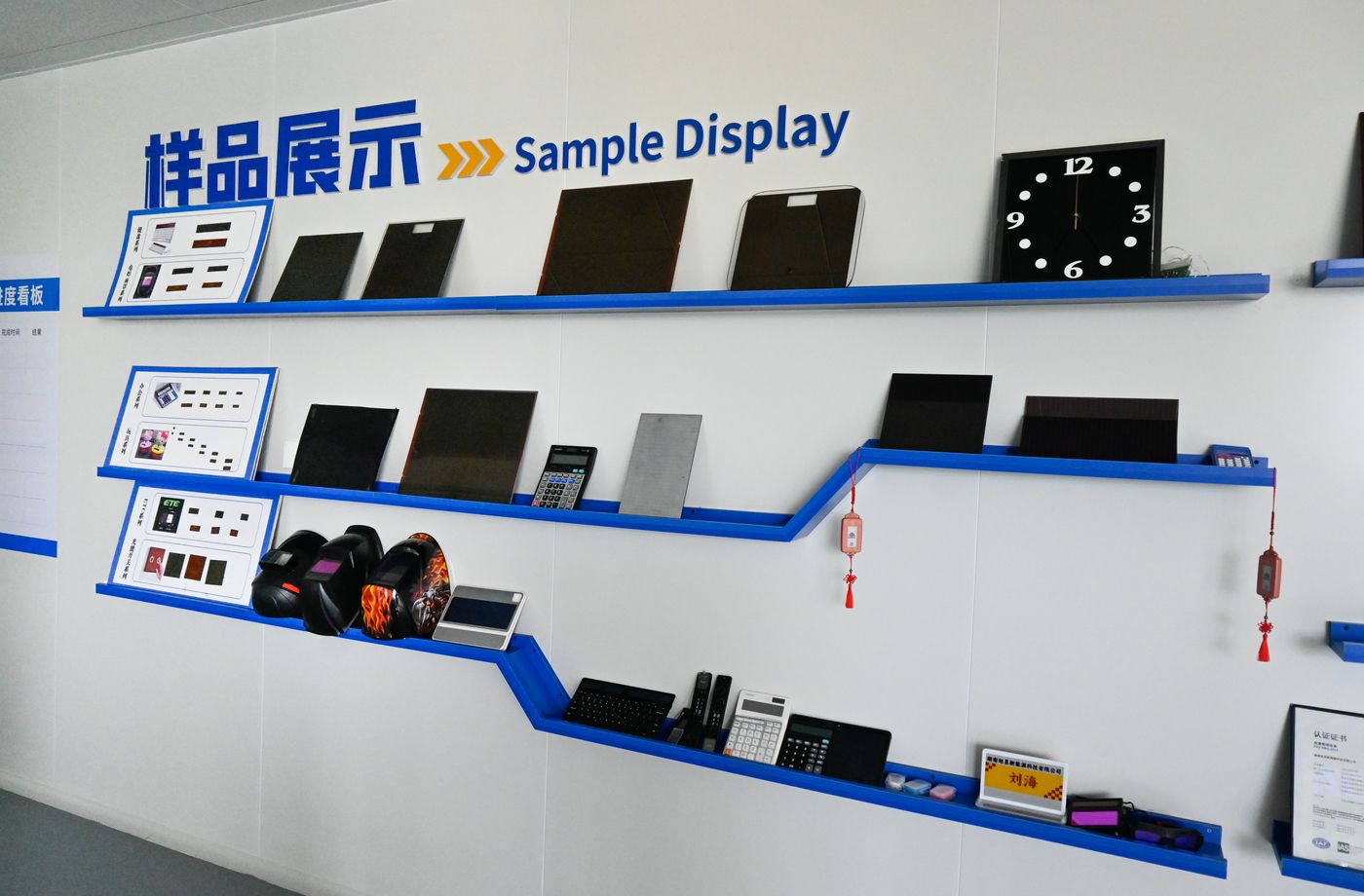
Our showroom displays a-Si thin film module samples in various sizes and forms, together with certificates and honors.
For product listings and quotations, please visit our 1688 factory store1688.com is a Chinese-language B2B platform. You can also call us directly.
Go to 1688 StoreFor product inquiries, samples and cooperation, please call us.